
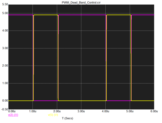
In a half-bridge or full-bridge MOSFET driver circuit, high-side and Low-side switches should not be turned on simultaneously for the system’s proper and safe functioning. Due to the propagation delay in driver circuits, both side switches may turn on for a short period. During this short period, a high current flows through the switches, and it causes the Bridged supply to be short-circuited. A waveform of a Half-Bridge control signal without a dead band is depicted in Figure (1).
Figure(1)
To avoid this potentially destructive high current flowing through switches, the turn-on period of the switches should not be overlapped at any time. A delay between ON conditions of the switches can be implemented, and this delay is called Dead-Band. In the Dead-Band period, both switches should be turned OFF. The Dead-Band period should be greater than the transition delay of switches from the HIGH state to the LOW state. When one switch was completely turned off, then the other switch turned on.
A lot of single-chip driver solutions with dead-band control are available on the market. But here, the objective of this article is to implement and simulate a Dead-Band control circuit using some basic building blocks to understand the hardware used in Dead-Band control circuitry. A simple circuit is shown in the Figure(2).
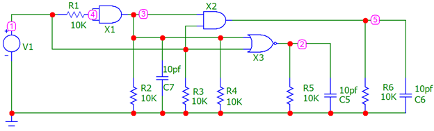
Figure-2
V1 : Pulse generator (0-5V)
X1 : AND Gate (74HC08)
X2 : AND Gate (74HC08)
X3 : NOR Gate (74HC02)
In the above circuit, A pulsed signal of 5V p2p is generated at node 1, and this signal is given to AND Gate X1 through resistor R1. R1 is to create a propagation delay between node one and node 3. Gates have their own propagation delay time, but that is not sufficient for High Voltage and High Current switches. Also, it is not adjustable, so R1 is used to set the propagation delay as per the required switches. The propagation delay between node one and node three with R1=10k is shown in Figure (3)
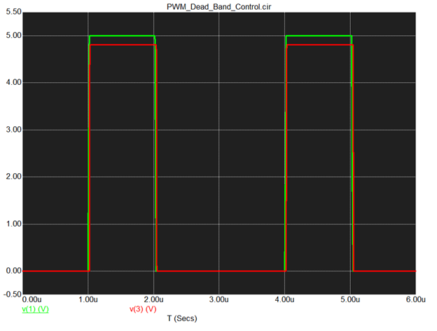
Figure-3
Now, the original signal at node 1 and the delayed signal at node 3 are given to X2 and X3 gates to achieve the proper driver signal with Dead-Band.
Nodes 2 and 5 give the final control signal.
Figure(4)
Propagation delay with R1=5k is shown in figure(5)
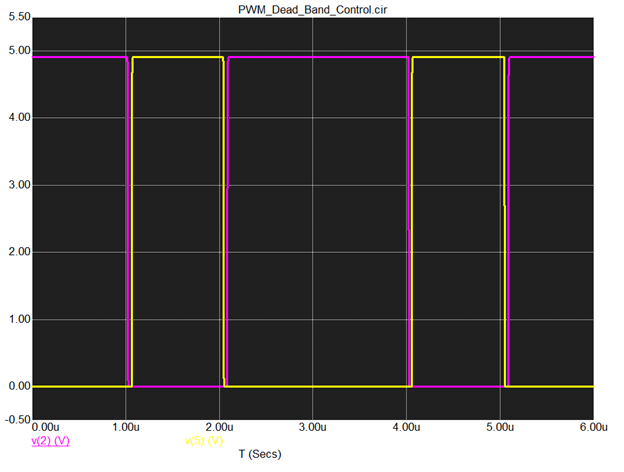
Figure(5)
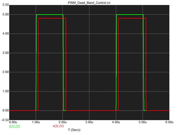
Propagation delay with R1=10k is shown in figure(6)
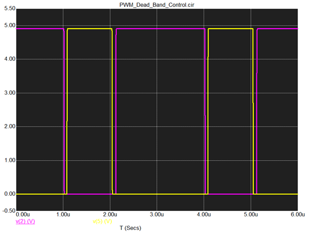
Figure(6)
Propagation delay with R1=22k is shown in figure(7)
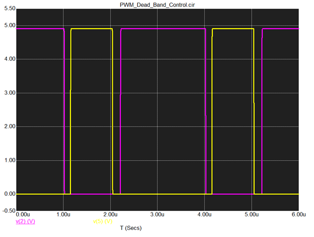
Figure(7)